| Nanowires Grown by Beam Epitaxy |
|---|
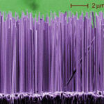
 Registration: Open to all. Date: December 4, 2008 Time: 11:00 am Venue: Centre for Solid State Physics, University of the Punjab, Quaid-e-Azam Campus, Lahore Abstract: Semiconductor nanowires (NWs) are attracting wide interest due to their unique physical properties and potential for application in nanodevices. NWs can be obtained by a number of growth methods, and their highly anisotropic growth originates by the presence of a metal particle, the catalyst, that determines the position and the diameter of the nanostructure. The most widely used catalyst is gold. The growth mechanism of catalyst assisted nanowires involves the incorporation of material both impinging on the catalyst particle and diffusing from the free substrate surface to the sidewalls of the wire. The interplay of these two phenomena is critical especially for the growth of alloy semiconductor compound NWs and one dimensional (1-D) heterostructure. Difference in the surface mobility between the constituents could give compositional inhomogeneities in alloy NWs and degradation of the interface sharpness in 1-D heterostructure. The systematic presence of a metal particle at the NWs tip could be exploited in single NW devices. Moreover, one of the most interesting characteristic of the III-V NWs grown by catalyst assisted self assembling is the peculiarity of having an hexagonal lattice structure (wurtzite), while their bulk and epitaxial parent materials have the cubic structure (zinc blend). In our laboratory we have synthesized GaAs NWs by molecular beam epitaxy (MBE) either using a thin gold, manganese, Ga layer as the growth catalyst or without any catalyst. In this talk some of the basics of NWs, their growth and potential applications will be covered.
Resource Persons:
Presenter Fouzia Jabeen Elletra Synchrotrone, University of Trieste, Italy Announcement Poster: Event Poster |
The LHC Computing Grid »

